Plasma etches trenches a nanometer wide. One slip, and your multi-billion-dollar AI chip design turns to scrap. We’re inside TSMC’s Fab 18 right now — or at least, as close as outsiders get — watching the alchemy that powers every ChatGPT query.
Zoom out. NVIDIA’s market cap just hit $3.2 trillion on the back of H100s and Blackwell chips. But those aren’t accidents. They’re the culmination of decades chasing hardware that can actually crunch matrix multiplications at warp speed. Forget algorithms for a second. Here’s the data: GPU compute efficiency for AI workloads leaped 300,000x since 2006, per Stanford’s hardware surveys. That’s not software tweaks. That’s silicon evolution.
And.
It’s fragile as hell.
How Do You Even Design an AI Chip?
Start with RTL — Register Transfer Level, the hardware’s poetry in Verilog or VHDL. Engineers describe logic gates, pipelines, tensor cores like architects sketching skyscrapers. But unlike software, you can’t iterate fast. Simulation alone for a 100-billion transistor chip? Months on server farms. One bug in the memory hierarchy, and your chip thermal-throttles under load.
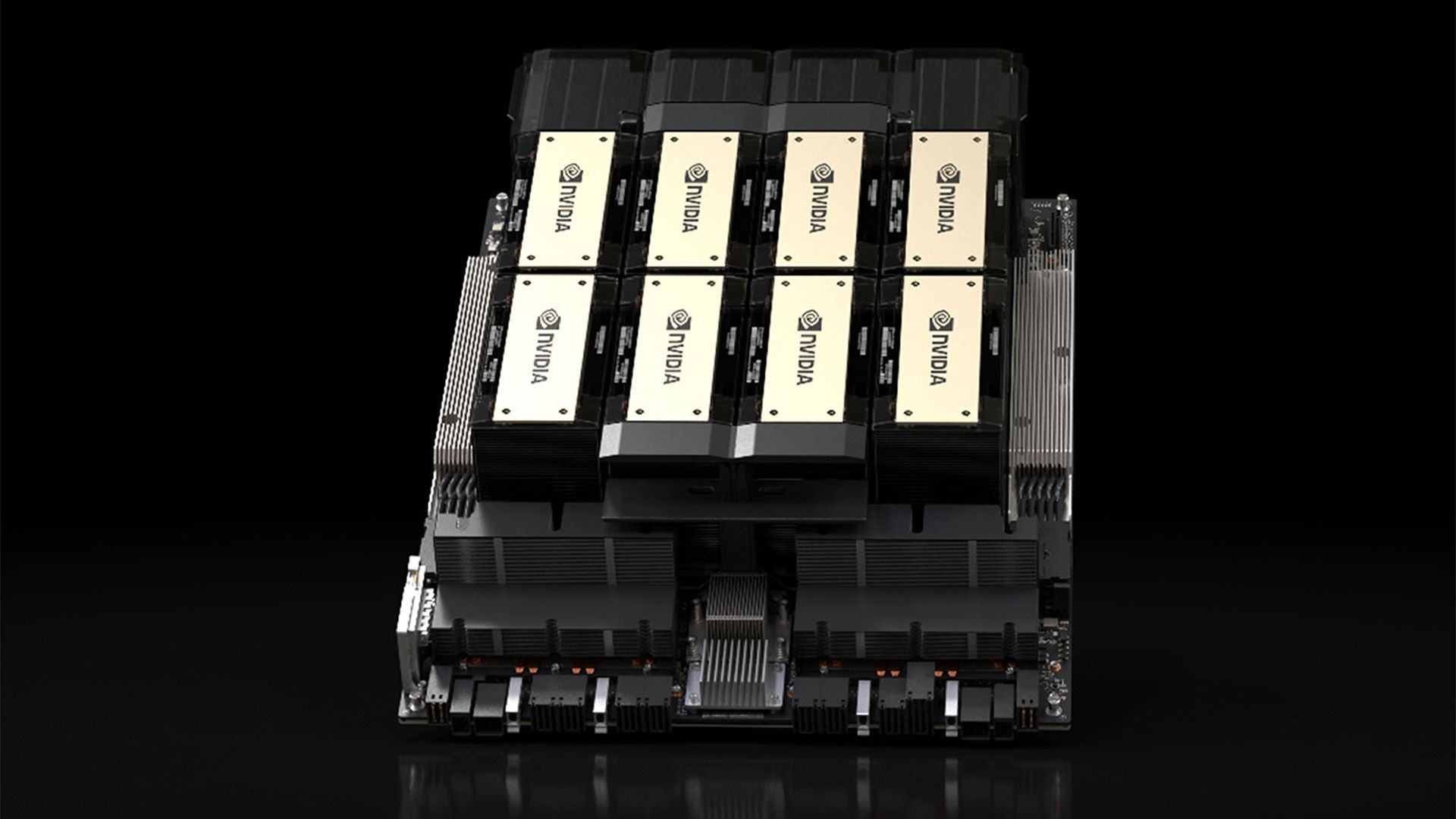
Take NVIDIA’s A100. It packs 54 billion transistors, optimized for FP16 precision where AI lives. Custom ASICs from Google or Amazon? They’re narrower — hyperscalers tune for inference, shaving 30-50% power versus training beasts. Market dynamic: Custom chips now snag 15% of the $100B AI accelerator pie, up from zilch five years ago, says TrendForce.
Let me tell you something that took me an embarrassingly long time to truly internalize: the reason deep learning works as well as it does in 2026 is only maybe 40% algorithms. The rest is hardware.
That’s from the original deep dive sparking this piece. Spot on. But here’s my twist — it’s more like 60/40 now, as models balloon to trillions of parameters. GPUs were a fluke; Quake-era rasterization accidentally nailed parallel floats.
Why GPUs Conquered AI — And Why Custom Chips Are Fighting Back
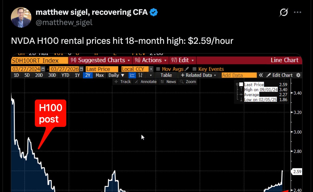
NVIDIA owns 80-90% of AI training silicon. Revenue? $60B last quarter alone. CUDA lock-in keeps devs hooked. But cracks show. Tesla’s Dojo chips promise 4x throughput on video data. Broadcom’s for Meta? Rumored at 10 petaflops per card.
Physics bites back, though. Dennard scaling died in 2006 — you can’t shrink clockspeeds and voltages forever without quantum tunneling ruining your day. Enter chiplets: AMD’s MI300X glues 146 tiles together, dodging monolithic yield drops. Yield rates? Industry secret, but whispers say 40-60% for 3nm nodes. That’s why H100s cost $30K a pop.
Look. Custom silicon makes sense for scale — hyperscalers burn billions on inference farms. But for startups? Rent GPUs. The capex math doesn’t pencil unless you’re deploying 100,000+ units.
Brutal truth: NVIDIA’s moat is software, not just hardware. CUDA’s ecosystem took 15 years to build. Challengers like AMD’s ROCm lag, adoption under 10%.
The Tape-Out Ordeal: When Code Hits Silicon
Tape-out. That moment you ship GDSII files to TSMC or Samsung. No take-backs. First silicon? 6-9 months later, $50-100M down. Then validation: Probe cards test billions of nets. One fab cycle failure? Rewrite RTL, tape out again. Multiply by 3-5 spins.
Extreme short: Heat.
AI chips guzzle 700W+. Junction temps hit 105C. Cooling? Liquid nitrogen for records, but data centers settle for immersion or fancy heatsinks. My bold call — photonics integration by 2030 halves power, echoing fiber optics’ telecom takeover in the ’90s. Lasers on chip for all-to-all interconnects. Historical parallel: Just as fiber killed copper bottlenecks, silicon photonics slays copper I/O limits.
But hype alert. Cerebras’ wafer-scale monsters? Impressive demos, but real-world yields suck for production. PR spin: “World’s largest chip!” Reality: Niche for DoD sims, not cloud scale.
Can AI Chip Supply Chains Hold Under Boom Times?
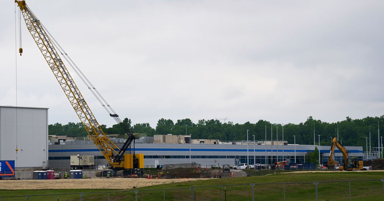
TSMC’s at 90%+ capacity on CoWoS packaging — advanced 3D stacking for HBM memory. Bottleneck city. US CHIPS Act pumps $52B, but Intel’s 18A node slips to 2025. Geopolitics? Taiwan quake risks 20% global output.
Data point: AI chip demand doubles yearly through 2027, per McKinsey. Prices? Stable for now, but shortages loom if Blackwell ramps slow.
Skeptical take: Everyone’s piling in — Apple, Huawei, even Samsung fabs. But physics caps nodes at 1nm-ish. After that? Carbon nanotubes or 2D materials. Don’t hold your breath; molybdenum disulfide prototypes are years from volume.
One paragraph wonder: Innovation’s real frontier isn’t bigger chips. It’s software-hardware co-design — training frameworks that exploit sparsity, reducing compute 10x without accuracy loss.
And here’s the editorial line: Betting against hardware progress is dumb. We’ve closed the GPU gap spectacularly. Next decade? ASICs everywhere, but NVIDIA prints money till someone cracks open-source stacks.
🧬 Related Insights
- Read more: CORPGEN’s Digital Employees Master Office Multitasking
- Read more: KV Caches: The Hidden Speed Boost Powering Your Daily AI Chats
Frequently Asked Questions
What is tape-out in AI chip making?
Final design handoff to the fab — GDSII files etched into silicon. No edits post-tape-out; first chips arrive months later.
Why are AI chips so expensive to produce?
Nanometer-scale fabs cost $20B+. Low yields on complex designs mean half your wafers are trash. Add HBM stacking.
Will custom AI chips kill NVIDIA’s dominance?
Not soon. CUDA ecosystem too sticky. But hyperscalers grab 20-30% inference share by 2028.