Everyday buyers of laptops, phones, even cars feel chip shortages in wallet-pinching delays and price hikes. Now, imagine fabs churning flawless silicon on first try, costs plummeting 20-30% over time—that’s the promise from VLSI 2025’s digital twin breakthroughs, starting with Intel’s 18A node.
Look, Intel’s pushing 18A hard to claw back foundry leadership from TSMC. But here’s the data: development cycles stretch to 3-5 years per node, burning billions. Digital twins? They virtualize the mess from atomic bonds to full fab lines, potentially halving those risks.
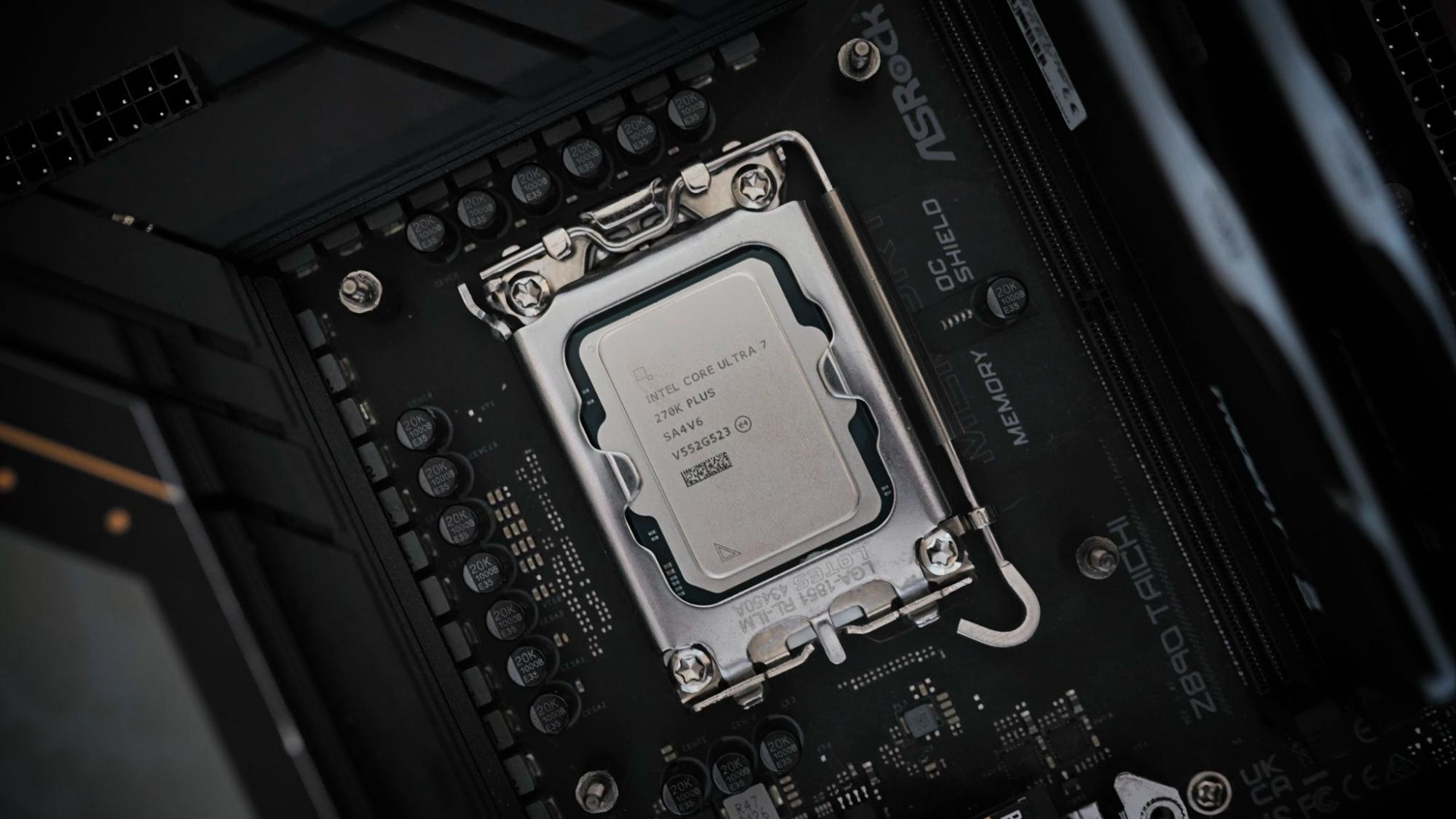
Intel 18A: Cost Realities Hit Home
Intel spilled 18A beans—RibbonFET transistors, PowerVia backside delivery, targeting 2025 ramps. Cost? Expect $20-25k per wafer start, per analyst whispers, versus TSMC N2’s $18-20k. Sharp edge: Intel claims 15% density leap over 20A, but yield ramps decide if consumers see sub-$1000 AI PCs sooner.
And backside power—burying signals under transistors—cuts voltage drop 20-30%, per simulations. But adoption? TSMC skips it for N2, eyes A16 maybe. Intel goes all-in. Smart, or desperate?
“GPU accelerated DFT-NEGF demonstrated a 9.3x speedup using only 4x A100 vs CPU, while Machine-Learned Force Field simulation… demonstrated near-DFT accuracy with 17 min compute cost vs 12 days.”
That’s Synopsys on atomic twins—game for gate stacks in 18A’s GAA shift.
Short para: China’s FlipFET steals headlines too.
FlipFET—vertical channels flipped for density—promises 1.4x area shrink over nanosheets. SMIC’s testing, dodging US bans creatively. Risk for West? Supply chain jitters if it scales.
Will Digital Twins Make Fabs Lights-Out?
Scale up. Lam’s SEMulator3D virtualizes wafers, exploding process combos under “Lam’s Law.” FinFET to GAA? Exponential nightmare solved pre-silicon. Etch profiles tuned virtually, stress strains mapped—widens windows 2x.
Fab-wide? Orchestrate 1000+ tools real-time. Predictive maintenance via embedded sensors catches drift before yields tank. Lights-out fab—no humans, 24/7 max output. Boeing-esque: their flight sims cut training crashes 90%; semis could slash dev costs similarly.
Unique angle—call it my Bloomberg hunch: digital twins echo 1980s CAD revolution for PCBs, which dropped design time 80%. Here, Intel 18A leans heavy; if twins deliver 10x sim speed, Intel Foundry grabs 20% AI chip market by 2027. TSMC lags? Nah, they’re copying fast.
But hype check. Atomic DFT’s pricey—GPUs help, but exascale needed for full GAA. ML force fields approximate; real silicon bites back.
4F2 DRAM vs 3D: Density Wars Heat Up
DRAM hits 1x nm wall. 4F2 planar? Scales to 10F2 logic density parity, but leakage kills it. 3D stacking—channel holes vertical—wins long-term, per VLSI data. Samsung, Micron push 3D; planar clings for cost.
Market math: AI servers guzzle HBM, but commodity DRAM? 3D cuts bit cost 30% at 1zb scale. Winners: stacked architectures, unless 4F2 ekes EUV tricks.
Interconnects next. Backside power spreads signals wider, resistance drops 50%. But not everywhere—memory skips it, logic first. Intel yes, TSMC selective.
Wander a bit: VLSI buzzed fab twins too. Lam’s plasma sims uniformize chambers; yield jumps 5-10%. Real people win—stable supply, no 2021 shortage redux.
Skepticism spike. Intel’s 18A PR spins flawless ramps; history says 18 months debug. Digital twins mitigate, sure—but atoms defy sims sometimes.
Why Does Backside Power Matter for Your Gadgets?
Power delivery’s bottleneck. Frontside? Congested. Backside frees 20% routing. IR drop halves; chips clock 10-15% higher. Phones thinner, laptops 2hr extra battery.
TSMC balks early—process pain. Intel risks it for AI edge. Data point: imec sims show 25% perf boost. If yields hit 80% fast, Intel surges.
China’s play—FlipFET sidesteps nanosheets, cheaper etch. Geopolitical twist: if viable, erodes West monopoly.
Deep dive payoff. These aren’t toys; trillion-dollar semi market pivots. Consumers? AI inferencing in $300 phones by 2026, if twins pan out.
Fab orchestration—virtual twins predict tool fails, uptime 98%. No more idle $500M lines.
Position clear: Twins must-have, Intel 18A viable if costs bend. Ignore PR; watch Q4 yields.
🧬 Related Insights
- Read more: AMI Labs Emerges from Stealth: Europe’s Bet on Physical AI Over AGI Hype
- Read more: Microsoft’s Responsible AI Standard: Principles Meet Practice
Frequently Asked Questions
What is Intel 18A process?
Intel’s 1.8nm node with RibbonFET and PowerVia, aiming 2025 production to rival TSMC N2 for AI chips.
Will backside power become standard in chips?
Likely for high-end logic by 2027, but memory and low-cost skip it—TSMC selective, Intel aggressive.
Future of DRAM: 4F2 or 3D?
3D stacking dominates post-1x nm for density and cost; 4F2 fades unless EUV magic.