Picture this: the chip world’s been buzzing with dread for Intel. Foundry losses piling up—$10 billion last year alone—while TSMC laps them on every AI node. Skeptics wrote Intel off as yesterday’s news, a relic clinging to x86 glory amid the ARM and custom silicon surge.
Then—bam. Reports hit that Intel’s in deep talks with Google and Amazon to package their beastly AI processors using EMIB-T, the next-gen bridge tech rolling out this year. Expectations? Intel scraping by on government handouts and Altera scraps. Reality? Billion-dollar packaging deals that could juice external revenue like never before.
This isn’t just a win. It’s a paradigm flip. Remember when transistors ruled the roost? Silicon shrinking smaller, faster, forever? Yeah, that’s over. Now, it’s about jamming monster multi-die systems together without melting or bottlenecking—enter advanced packaging as the unsung hero of AI’s explosion.
The Bridge to AI Billions
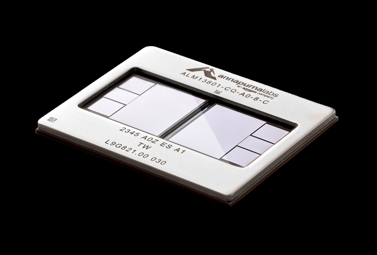
Intel’s EMIB (Embedded Multi-Die Interconnect Bridge) isn’t new—it’s been gluing chiplets since 2017. But EMIB-T? That’s the turbo version, punching through-silicon vias right into the bridge for killer power delivery and signals zipping across massive 120x180mm packages. Up to 38 bridges, 12+ reticle-sized dies. Hyperscalers like Google (TPUs) and Amazon (Trainium, Inferentia) are starving for this to scale their AI monsters beyond single-die limits.
Here’s the quote that nails it, straight from Intel Foundry head Naga Chandrasekaran to WIRED:
“Even more so than the silicon itself, chip packaging is going to transform how this AI revolution comes to fruition over the next decade.”
Spot on. And CFO Dave Zinsner? He’s teasing “deals in the billions of dollars per year” on packaging alone, eyeing 40% margins matching Intel’s core biz.
But wait—unique twist I haven’t seen elsewhere. This echoes the 1980s DRAM wars, where Intel bailed on memory to double-down on CPUs, letting Japan dominate fabs temporarily. Packaging today? It’s Intel’s shot to reclaim the high ground, not by out-noding TSMC (impossible short-term), but by becoming the indispensable glue for everyone else’s silicon. Bold prediction: if these deals land, Intel Foundry hits breakeven by 2027, fueling 18A ramps without more CHIPS cash begs.
Why Hyperscalers Can’t Ignore EMIB-T
Google and Amazon aren’t chatting for fun. Their custom AI silicon—think Trillium waves or Trainium3—is hitting thermal and I/O walls. Single chips? Cute for laptops. But training GPT-6 equivalents? You need chiplet cities, interconnected at blistering speeds, without the latency tax.
EMIB-T delivers. Foveros stacks vertically for density; EMIB-T bridges horizontally for scale. Intel’s ramping fabs worldwide: New Mexico’s Fab 9 (CHIPS-funded beast, live since January), Penang nearly done (99%—Malaysian PM confirms first ops this year), even outsourcing to Amkor in Korea. Portugal and Arizona next. Capacity explosion.
Contrast Intel’s packaging optimism with its Q4 bloodbath: $4.5B revenue, $2.5B loss. Full-year foundry? $17.8B in, $10.3B out. External foundry? Pathetic $307M. Packaging’s the lifeline—Zinsner bumped forecasts from hundreds of millions to “well north of $1B.”
Will Intel’s Packaging Deals Actually Close?
Look, hype’s thick here. Intel, Google, Amazon—all mum. Sources say “ongoing talks,” not signed checks. Zinsner’s “close to closing” echoes every foundry sales pitch since forever. And history? Intel’s external foundry wins have been meh—Microsoft dipped toes, now Microsoft’s Broadcom-bound for Cobalt.
Yet—energy’s different. AI’s pace demands it. Amazon’s not building packaging fabs; neither’s Google. TSMC’s CoWoS is slammed (Taiwan quake drama didn’t help). Intel undercuts on geo-diversity, CHIPS subsidies, and—crucially—EMIB-T’s edge over CoWoS for certain topologies. If not billions, it’s still a foothold.
Skepticism check: Corporate spin screams loud. “Transform the AI revolution”? Please. But numbers don’t lie—packaging revenue’s real, scalable, high-margin. Intel’s not pretending to beat TSMC at nodes; they’re pivoting smart.
The Global Fab Frenzy
Rio Rancho. Penang. Songdo. It’s a packaging empire rising.
New Mexico’s $500M CHIPS glow-up turned Fab 9 into an EMIB/Foveros powerhouse. Malaysia’s Penang? Intel CEO Lip-Bu Tan briefed the PM—ops later this year. First-time Amkor outsource in Korea seals volume bets.
This matters because AI clusters aren’t US-only. Supply chain snarls killed plenty dreams; Intel’s multi-continent play dodges that.
And the wonder? Imagine: your next TPU or Trainium, not a monolithic slab, but a towering metropolis of dies, bridged by Intel magic, powering wonders we can’t yet dream.
Why Does Packaging Trump Silicon Now?
Short answer: physics.
Moore’s Law? Drove nodes to 2nm, sure. But AI workloads? Parallelism explosion. One die can’t hack 1000x tokens. You stack, bridge, pool—like Lego on steroids, but at 1μm pitches.
Intel’s playing 4D chess. While Nvidia hoards Blackwell, Intel feeds the ecosystem. Prediction: by 2028, 30% of AI packaging flows through Intel, starving TSMC’s queue.
Hype? Some. But this feels real. Intel’s foundry survival hinges here—not 18A magic, but glue for the AI multiverse.
**
🧬 Related Insights
- Read more: Amazon Bedrock’s AgentCore Gateway: The Magic Adapter Plugging AI Agents into Enterprise Tools
- Read more: Google’s Gemini API Splits into Flex and Priority: The Real Cost of Reliable AI
Frequently Asked Questions**
What is Intel EMIB-T and how does it work?
EMIB-T upgrades Intel’s bridge tech with through-silicon vias for better power and signals in huge multi-die AI packages—up to 120x180mm, 38+ bridges.
Will Intel’s packaging deals with Google and Amazon happen this year?
Talks are hot, production ramps now—CFO says billions incoming—but no signatures yet; expect announcements post-fab quals.
Can Intel compete with TSMC in advanced packaging for AI?
Not everywhere, but EMIB-T’s unique for certain scales, plus global fabs and CHIPS edge give a real shot at 20-30% market slice by decade’s end.